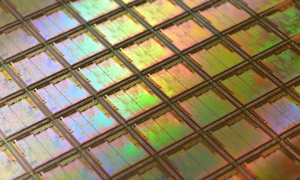
Intel continues to work on improving the yield per wafer for its 10nm process, but without neglecting one of its key long-term goals, the leap to the 7nm process, something that, according to several sources, could be completed within a few years.
One of the first consumer architectures Intel will bring to market based on the 7nm process is known by the code name Meteor Lake, and if all goes according to plan, it is expected to be the successor to Alder Lake, the last architecture Intel will develop based on the 10 nm process.
But in case any of them gets lost, I remind you that the Intel roadmap for the 10 nm process is configured as follows: Cannon Lake (10nm), Ice Lake (10nm+), Tiger Lake (10nm++) and Alder Lake (10nm++).
To make the leap to the 7nm process, Intel still has one important goal to achieve, which is to make the 10 nm process profitable. The Santa Clara-based company has invested a lot of resources in this manufacturing process, and its time to market has certainly been very limited, so it is clear that it still has a lot to say.
We will see how Intel’s roadmap develops over the next few terms, and especially when they decide to launch their first generation of processors in 7nm technology. They will probably decide to adapt it to the specifics of the 10 nm process, so it may well go beyond 2022 and we may have to expect a delay.
According to the latest leaks, Intel’s 7nm manufacturing process is far ahead of TSMC’s 5nm manufacturing process because it enables much higher transistor density. It makes sense because both processes are used to make very different chips and it is a reality that we have already seen in the 10 nm process.
Intel once said that they had learned from the mistakes of the 10 nm process and had adopted all the necessary tools for an optimal transition to the 7nm process, including the use of extreme UV lithography, which means that the process should have a higher success rate per wafer in the initial phase and be economically and technically feasible in a shorter time.
