


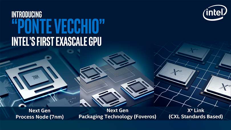
It is rumored that Intel is preparing its next-generation Xe graphics architecture Intel DG2 GPU with the base of TSMC’s 7nm process node. While Intel has already introduced its Xe Low Power ‘DG1’ GPU and the Xe HPC ‘Ponte Vecchio GPU’, the only missing product is the high-end Xe or better known as DG2.


Intel Xe DG2 is now in production on 7nm TSMC
There is likely to be a lot of rumors and information about Intel’s Xe DG2 GPU, as it first appeared in test controllers last year along with the DG1 GPU. There were no details other than the apparent EU count of the three variants that were revealed, and the fact that the DG2 uses the Xe HP (high-performance microarchitecture) instead of the Xe LP (low-performance architecture), which is more suitable for entry-level designs like the DG1 GPU.
AdoredTV reports that they have received information that Intel will introduce its DG2 GPU in 2022, based on the 7nm process node. More interesting, Intel will use the TSMC nodes to produce the DG2 GPU, rather than its own 7nm EUV technology.
Intel will manufacture its high-end DG2 GPU at TSMC’s 7nm [Rumor]

This way Intel would rely on TSMC’s 7nm process, not the 7nm+ process that EUV has. TSMC’s 7nm+ EUV process reached production volume in Q2 2019, which could be the other reason why Intel is using the standard 7nm path instead of its own 7nm node (EUV) or TSMC’s 7nm+ node, as the associated costs are much higher.