

The technological industry is in continuous transformation and improvements. At the moment in the market, we can find transistors of different sizes. So being one of 14 nanometers is the one that is the working technology nowadays. This measurement of nanometer is a value that indicates the distance between transistors and each one is equivalent to one million nanometers.
However, there is a company willing to overcome it more. However, this may seem impossible. But IBM has announced a new chip at the size of a nail with transistors of 5 nm. So making a record for the smallest to date in the world. It seems that Moree ‘s Law is not dead and will be fulfilled. Although it is true that in recent years it had slowed down.
5 nm Transistor Technology Moor’s Law
The Moore ‘s Law has been rather difficult to maintain over the past three years due to complications begins to present silicon transistors to be reduced to such small sizes. Now, IBM has introduced the first 5-nanometer chip. Which ensures stability in the industry for at least 4 years.
If two years ago, the New York-based multinational technology company surprised us by working on the first 7-nanometer chip with capacity for 20 billion transistors. And now we have learned that it is developing the smallest transistor in the world.
Each transistor is used to handle zeros and ones. So that is the basic units in computer science. The greater number of transistors on a chip, the greater processing power. The manufacturer along with its two partners Global Foundries and Samsung is in the midst of manufacturing the smallest transistors ever seen. It is the same equipment that launched the chip of 5 nm. Whose commercialization is predicted for 2019?
As for the model that will follow, we have known that the new IBM chip will be of 5 nm. And will increase its capacity allowing some 30 billion transistors. We also know that it will have the same ultraviolet extreme lithography (EUV) that counts the 7 nm. But the appearance will not be the same.
FinFET architecture for 5 nm Transistor Technology
The design of the newest transistor in the world of IBM will feature a new structure built with a stack of four silicon nanowires. So leaving aside the FinFET architecture that is the one they are working since 2011. As its name suggests, transistors are in the form of a fin. It comes with three current transport channels surrounded by an insulating layer. The disadvantage of FinFET technology is that it collides with the physical dimensions of the chip. that is why IBM has decided to opt for another.
The 5 nm chips will allow sending signals through four doors, instead of three that allowed FinFET. Thanks to the already used extreme ultraviolet (EUV) technology. By using this technology the finer details are created on the chip.
40 percent increased performance in 5 nm Transistor Technology
In addition, the 5 nm transistors will improve the performance by 40% on fixed power. And will provide a 75% energy saving in matched performance.
This new release from IBM could set the precedent for the future of mobile devices. It is something that Samsung is working on and also Huawei for increasing the battery of current devices. Something for which we will still have to wait for the previous model, the 7 nm is not expected to reach the market until 2018. So that the new IBM model of 5 nm would move to the position of the smaller transistor to the Date, although it would not be ready until minimum 2020.
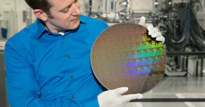
The new 5nm (nanometer) IBM chip will hold up to 30 billion transistors. This involves a new processor with such a quantity of transistors in the space that a fingernail would occupy. That is summarized in a decrease of 2 nm and an increase of 10 billion transistors with the previous chip.
This technology is achieved by the use of silica nanoparticles. That would reduce the space by increasing the yield. So this is something that can not be achieved by the FinFET structure. This is because, in the latter system, only the space between the fins could be reduced.
Technology Advancements by 5 nm Transistor Technology
This method involves the return to a two-dimensional system. And an optical lithography with very short wavelengths (13.5 nm). That will be used together with extreme ultraviolet lithography (EUV ). At the moment, no one in the industry knows what will come after 3 nanometers. The arrival of three-dimensional chips solved the problem of two-dimensional structures in which the channel was so small that atoms could not transport electricity fast enough. FinFET arranged it by adding three-dimensional channels.
2D System
Now, IBM has returned to the two-dimensionality of the hand of Samsung and Global Foundries. That is by using a horizontal structure, compared to the vertical of FinFET. The GAAFET method used by IBM consists of three nanowires one above the other above the drain and the source, with the door (the bit part that activates and deactivates the channel) between the gaps. With this, a greater volume of door and channel is achieved, making GAAFET more reliable, with better performance, and with an even better scalability that allows reaching the 3 nanometers.
5 nm Technology will come in 2019
While the 10-nanometer chips have just hit the market with Snapdragon 835 and Exynos 8895. Also, other industry players such as Intel have not yet taken the plunge. Even NVIDIA will use the 12 nanometers for Volta, that is its new generation of graphics cards. Subsequently, at 10 nanometers we will reach 7 nm in 2019. And now IBM has just said that after 7 nm we will reach 5 nm. Although these will not arrive for at least four years.