

It appears that in transistor maturing technology Moore’s law is not respected. We see developments on exponential scales. Currently, the wafer engraving process involves 7nm. And many well-known companies are doing their best to introduce their latest technologies, e.g. AMD, which outsources 7nm via TSMC. However, Intel is still in the background and does not rely on third parties.


Extreme photolithography of ultraviolet radiation (EUV) has long been presented as a lifesaver in the semiconductor industry: Modern manufacturing techniques have exploited their limits in drawing even smaller transistors on silicon wafers, EUV is a small revolution that allows much finer details to be engraved. After all, we are seeing the EUV coming onto the market this year, with an output of two hundred watts (much more soon).
EUV is used for 7 nm
Currently the EUV is used for 7 nm processes. Manufacturing has a relatively high number of errors compared to previous processes at the beginning of its professional activity. In fact, the photons used so far had a wavelength of 193 nm: with the EUV we go to 13.5 nm – and the energy of a photon is proportional to the opposite of its wavelength. The masks used (a design of the transistors to be produced: depending on whether the mask retains a photon or not, the silicon wafer is dug or not), therefore the photons must resist much higher energies than before. Today’s users suffer from a very special problem: they cause random defects (photons that happen when they shouldn’t or vice versa), “stochastic printing errors”.
A breakthrough for TSMC 5 nm and lower engraving process?
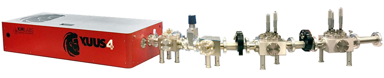
To solve the problem, IMEC (a Belgian company) and KMLabs (Americans) formed a team to create a very high-resolution EUV image laboratory. The system developed by them generates EUVs with very high-energy infrared pulses transmitted in a gas: The resulting EUVs are pulse sequences ranging from a few attoseconds (one billionth of a billionth of a billionth of a second) to a few picoseconds (one millionth of a millionth) with wavelengths between 6.5 and 47 nm.
This laser can be used for interferometry (process behind certain optical microscopes) in the micrometer range: It is possible to identify details in the order of eight nanometers. It can also observe molecular dynamics and ionization and thus help to understand the process of chemical processes. Practical experience? Many laboratories test photoresist masks with substrates of different materials, but they had no possibility to analyze their behavior during exposure.
On the other hand, this laser has extremely limited power: it could not (or only very slowly) be used to produce semiconductors. New developments ( relatively sizeable ) could expand the technology, but they would require several decades of development.