


At the Next Horizon conference earlier this month in San Francisco, Advanced Micro Devices (AMD) presented its new x86 processor architecture Zen 2, which will replace Zen+. The processors that will first benefit from this new architecture are expected to appear next year in the new generation of AMD CPUs for servers and workstations codenamed Rom processors that will replace the Zen-based EPYC CPUs.

Zen 2 landed with direct 7nm etching
The company took the opportunity to explain some details about the architecture. AMD has decided to ignore the 10 nm. Zen 2 will take advantage of TSMC’s 7 nm etching technology and allow AMD to make a huge leap from 12 nm to 7 nm directly. The 7 nm process developed by the Taiwanese smelter promises to halve consumption, double density and deliver 1.25 times the performance for the same power on the new chips that will operate it.

Amazing throughput without competition
AMD has made significant changes to Zen 2 to enable it to offer double the throughput of its first generation Zen architecture: a completely redesigned execution pipeline, large floating-point advances with 256-bit floating-point doubling and twice the bandwidth. One of the most important improvements for Zen 2 is the increase in core density by a factor of 2X, which allows the integration of up to 64 cores / 128 threads per chip and thus twice as much core complex (CCX) and die on the same package.

AMD’s new “Chiplet” design
AMD has made a number of improvements to Zen 2. In order to provide the extended delivery units with improved throughput and performance, it was necessary to adapt the front system. For this reason, the branch prediction unit was revised. These include pre-fetch improvements and several undisclosed optimizations of the instruction cache. The microoperation cache (µOP, the detailed low-level instructions used in some designs to implement complex machine instructions) has also been modified, including the µOP cache tags and the µOP cache itself, which has been enhanced to improve command flow throughput. The cache memory size at Zen was 2,048 entries. The exact details of the Zen 2 changes are not yet known.
Most backend changes concern floating-point units. The most important change is the extension of the data path, which has been doubled in width for floating-point execution units. This includes load/save operations and FPUs. In Zen, AVX2 is fully supported by the use of two 128-bit micro-operations per instruction. The load and save data paths also have a width of 128 bits. During each cycle, the FPU can receive 2 loads from the load/storage unit, each up to 128 bits. In Zen 2, the data path is now 256 bits. In addition, the execution units now have a width of 256 bits, so that 256-bit AVX operations no longer need to be divided into two 128-bit micro-operations per command. With 2 256-bit FMAs, Zen 2 is able to achieve 16 FLOP/cycle, which corresponds to the core of the Intel Skylake client.
First technical specifications published by AMD
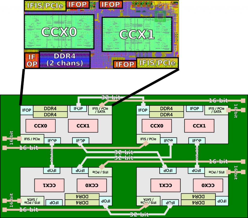
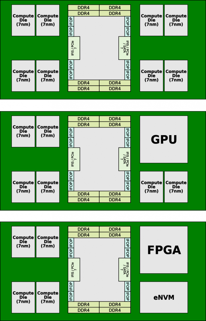
AMD’s second-generation EPYC is codenamed Rome, the successor to Naples. Both are suitable for sockets and platforms. Please note that Milan, the successor of Rome, is also compatible with sockets. Rome still uses a multi-chip approach to increase the number of cores, but the design of the system itself has changed dramatically compared to the previous generation. With Naples, AMD has expanded the design to 8 cores, the Zeppelin, to 32 cores by combining four of these SoCs through their exclusive Infinity Fabric connection. This process provided eight memory channels and 128 PCI (Peripheral Component Interconnect) channels distributed across all matrices.
An AMD Zen-based Epyc chip uses four matrices
With Rome, AMD goes even further. Building on what had begun with Threadripper 2, AMD provided Rom calculation matrices and an I/O matrix, but this time AMD removed the key execution blocks and moved them to new calculation matrices, taking advantage of the 7nm TSMC process and taking advantage of lower performance and density. The calculation matrices are then connected to a central I/O matrix that manages the I/O and memory. The chip is manufactured on a mature 14 nm process from GlobalFoundries.