

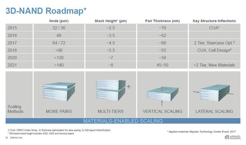
Sean Kang of Applied Materials spoke about the next generations of 3D NAND Flash at the International Memory Workshop (IMW) in Japan. The roadmap says that the number of layers in this type of memory should increase to more than 140, while the chips should be thinner.
3D NAND memory will reach 120 layers by 2020
In 3D NAND memory the memory cells are not in one plane but in several layers one on top of the other. In this way, the storage capacity per chip (matrix) can be significantly increased without the chip area has to be increased or the cells having to contract. Almost five years ago, the first 3D NAND, Samsung’s first generation V-NAND with 24 layers, appeared. In the next generation, 32 layers were used, then 48 layers. Today, most manufacturers have reached 64 layers, with SK Hynix leading with 72 layers.
The roadmap for this year speaks of more than 90 layers, an increase of more than 40 percent. At the same time, the height of a storage stack should increase by only about 20%, from 4.5 μm to about 5.5. This is because, at the same time, the thickness of a layer is reduced from approximately 60 nm to approximately 55 nm. The adaptations to the design of the memory cells and the CMOS Under Array (CUA) technology already used by Micron in 2015 are key features of this generation.
Kang’s roadmap sees the next step for 3D NAND in more than 120 layers, something that will be achieved by 2020. By 2021, more than 140 layers and a stacking height of 8 μm are forecasts, requiring the use of new materials. The routing does not deal with storage capacities.
Today, manufacturers have reached 512 gigabits per matrix with 64-layer technology. With 96 layers, 768 Gigabit will be achieved initially and with 128 layers finally 1024 Gigabit, so around a terabit is possible. Four-bit QLC technology per cell can also enable terabit chips with a 96-layer structure. Samsung wants to achieve this with the fifth generation of V-NAND and introduce the first 128 TB SSDs on this basis.