

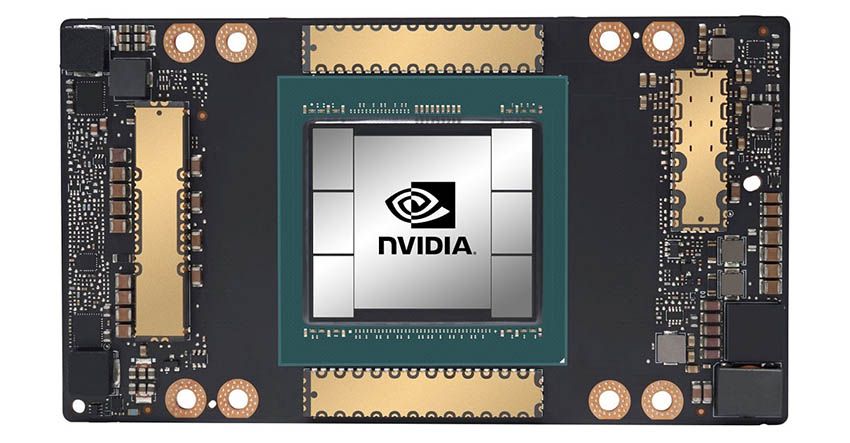
Following the announcement of the Tesla A100 GPU and the first details of Ampere, Nvidia has released a more complete version on the new architecture and specifications of the new Tesla A100-based GA100 GPU.
The most interesting information revealed in this blog is that the new Tesla A100 does not use the entire core, but only 7/8 of it. The full core has the following specifications:
- 8 GPCs, 8 TPCs/GPC, 2SMs/TPC, 16SMs/GPC, 128SMs per full GPU
- 64 CUDA cores FP32/SM, 8192 CUDA cores FP32 per full GPU
- 4 third-generation/SM cores, 512 third-generation cores per full GPU
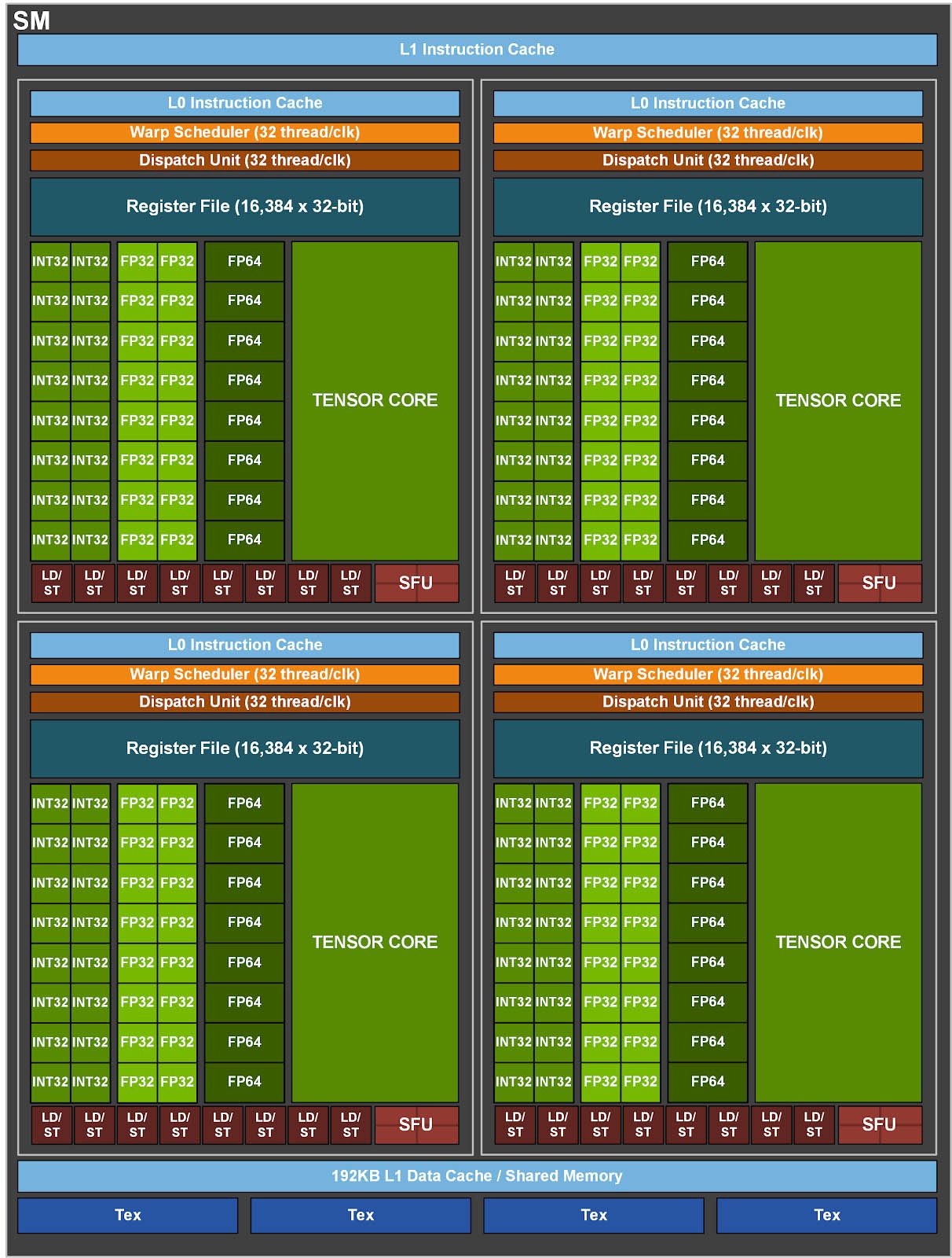

6 HBM2 memory stacks, 12 512-bit memory controllers
This allows us to have a 6144-bit bus and up to 48 GB of HBM2 memory with a bandwidth of up to 1.866 TB/s when using the same 1215 MHz HBM2 memory of the Tesla V100.
RT cores, raster units, video outputs, and NVENC encoders are not included because they refer entirely to artificial intelligence.
- The third-generation core sensor
- Acceleration for all data types, including FP16, BF16, TF32, FP64, INT8, INT4 and binary
- Tensor Cores’ TF32 operations provide an easy way to accelerate FP32 input/output data in deep learning and high-performance computing frameworks that run up to 10x faster than the
- Tesla V100 in FP32 FMA operations or up to 20x faster in scattered arrays.
- The FP16/FP32 mixed-precision core sensors provide unprecedented processing power for deep learning and run up to 2.5x faster than Volta core sensors and up to 5x faster in dispersed arrays.
- FP64 operations on Tensor Cors run-up to 2.5x faster than Tesla V100 DFMA FP64 operations.
- INT8 operations with scattered arrays provide unprecedented processing power in deep learning interference and run up to 20x faster than INT8 operations on Tesla V100.
- 192KB combined memory and L1 cache, 1.5x larger than a Tesla V100 SM
- New asynchronous copy instruction to load data directly from global memory to shared memory, optionally skipping the L1 cache and eliminating the need for an intermediate register file.
- New shared memory lock unit (asynchronous lock) to be used together with the new asynchronous copy instruction
- New instructions for handling the L2 cache and location checks.
New programming improvements to reduce software complexity
Without a doubt, Ampere brings great improvements, even if we haven’t seen the whole architecture yet, but only part of it. It is expected that Nvidia will also release RT Cores 2.0 and a new version of NVENC. So watch out for the announcement of the GeForce and Quadro versions in the second half of the year.