


The Intel Xe HP and Xe HPC are the crown jewel of the company’s GPU aspirations for data centers. On Intel Architecture Day 2020, the company gave us clear expectations, and the short answer is that the Xe HP provides metrics for standard computing.

This is the intellectual successor to Intel’s Larrabee program and the Xeon Phi product line, with the goal firmly focused on Nvidia’s A100 solution. In view of the exponential growth of the amount of data that needs to be processed, Intel is making every effort.
The Xe HP chips are also not used in consumer graphics cards. This task has been shifted to Intel’s Xe HPG, a GPU for enthusiastic gamers, which will omit the HPC (high-performance computing) element and add ray tracing hardware. The Xe HP will use Intel’s 10nm SuperFin process (which is actually the next step in the 10nm Enhanced SuperFin process), which is The new name for the “10nm ++” node that will be used for the upcoming Tiger Lake CPUs.
The Xe graphics architecture is designed to scale from trillions (i.e. consumer hardware) to trillions (i.e. supercomputers), with the Intel Xe HP / HPC as its successor. The basic design consists of a single block, as Intel’s monolithic GPU for vector and matrix calculations is called.
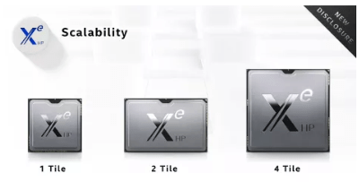
We’ll go into the specifications later, but the most important thing is that for the current generation it is via EMIB (Embedded Multi-Core Interconnect Bridge) and for the future Xe HPC Ponte Vecchio it is via Foveros (Core Stacking) and Co-EMIB, allowing Intel to scale from a 1-block implementation to a 4-block solution. Because of the high-speed connections, 1-block, 2-block, and 4-block solutions will be represented as single GPU instances, with the latter offering much higher performance.
We’ve seen several images of Xe HP over the last few months, and now we know exactly what each image represents. There are indications that the Xe HP is close to the maximum mark size for a microprocessor (about 850 mm2), with the 2-block package doubling, and then the 4-block package doubling again. The full-fat 4-block package measures about 60×60 mm – possibly even larger.
So what kind of hardware has Intel built into the Xe HP? First of all, each tile seems to contain two HBM2e stacks, potentially providing up to 32 GB RAM and 820 GB/s bandwidth. We don’t have any details about the clocks or the capacity Intel uses for the HBM2e stacks, but it seems to be at least 16 GB in total.